 The signing ceremony of Hebei Chemical Pharmaceutical Vocational Technology College's "Standing Enterprise Workstation" in our company was held at the headquarters of our company. Dean Chai Xiqing, deputy party secretary and deputy director Yue Xushui, Zhang Jijun, general manager of the company, Deng Dongkui and Jia Xiaochun, deputy general managers, and relevant department heads attended the signing ceremony.
 This “residential workstation†is another important measure for cooperation between our company and universities. In order to deepen the cooperation between our company and universities in a broader way, our company and the Hebei Chemical and Pharmaceutical Vocational Technology College adhere to the principle of “cooperative education, cooperative education, cooperative employment, and cooperative development†to tap their potential for superior resources and cultivate the needs of the company. Highly-qualified skilled and advanced technical application talents, to create a talent training model of “combination of school and enterprise, and integration of work and studyâ€. Both parties jointly develop and understand professional talent training programs, jointly determine training objectives, formulate teaching plans, adjust curriculum settings, undertake teaching tasks, and ensure the implementation of practical teaching. Hebei Chemical and Pharmaceutical Vocational Technology School also sent professional teachers to our company to produce first-line job training, and participated in technological transformation and new product development work to achieve the training and optimization of “dual-qualified†teachers.
The establishment of "stations with corporate offices" has created a new platform for the cooperation between our school and enterprises, and the realization of a win-win situation for schools and enterprises will surely promote more extensive and in-depth cooperation between our company and universities.
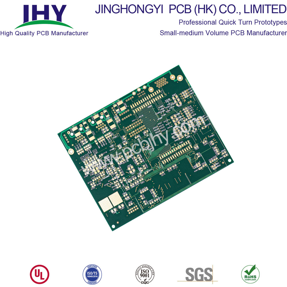
Cheap 12 Layers PCB stackup and thickness
We are one of the few manufacturers in China that can manufacture 12-layer PCB boards on a large scale.
The 12-layer board can usually be manufactured smoothly on a 1.6mm thick FR-4 board. But we've seen more 14- to 16-layer boards are being fabricated into 1.6mm thick boards, but the number of manufacturers that can produce them is limited to manufacturers that can produce HDI PCB boards. Those who can produce HDI Circuit boards are increasing.
12 Layers PCB– Heavy industry boards or boards with may tracks
For industrial PC design, 12-layer circuit boards are more popular. Compared with other multi-layer PCB circuit boards, such as four-layer circuit boards, 8-layer circuit boards, 10-layer circuit boards, The price of the 12-layer PCB is still reasonable.
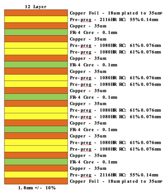
12 layer PCB stackup and thickness
12 Layer PCB Stack Up
Top Layer †18um Copper Foil (plated to 35um+)
Preâ€Preg †1 x 2116
Layer 2 & 3 †0.13mm Frâ€4 Core with 35um/35um Copper
Preâ€Preg †1 x 2116
Layer 4 & 5 †0.13mm Frâ€4 Core with 35um/35um Copper
Preâ€Preg †1 x 2116
Layer 6 & 7 †0.13mm Frâ€4 Core with 35um/35um Copper
Preâ€Preg †1 x 2116
Layer 8 & 9 †0.13mm Frâ€4 Core with 35um/35um Copper
Preâ€Preg †1 x 2116
Layer 10 & 11 †0.13mm Frâ€4 Core with 35um/35um Copper
Preâ€Preg †1 x 2116
Bottom Layer †18um Copper Foil (plated to 35um+)
Stardand 12 Layer PCB 1.6mm +/†10%
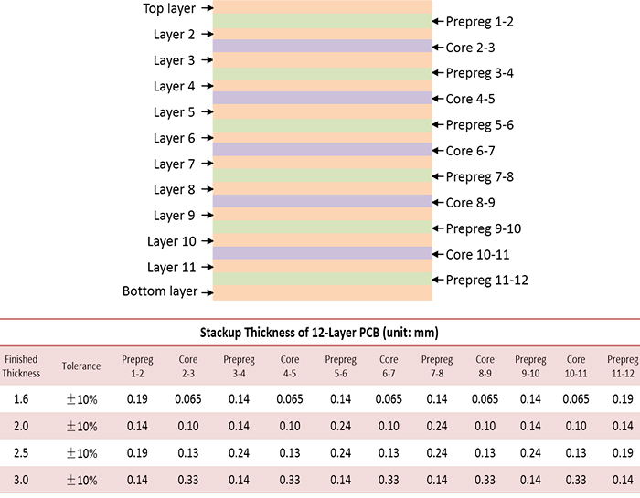
12 layer stackup – 4 GNDs
I use this stackup a lot, provides GND shielding of high speed signals and has tightly coupled Power-Ground planes:
Signal / Solid GND plane / High speed signals and important buses / Solid GND plane / Power / Power or Mixed with signals / Power or Mixed with signals / Power / Solid GND plane / High speed signals and important buses / Solid GND plane / Signal
12 layer stackup – two additional signal layers
Signal / Solid GND plane / Signal / Signal / Solid Power Plane / Power or Mixed with signals / Power or Mixed with signals / Solid Power Plane / Signal / Signal / Solid GND plane / Signal
12 layer PCB stackup thickness
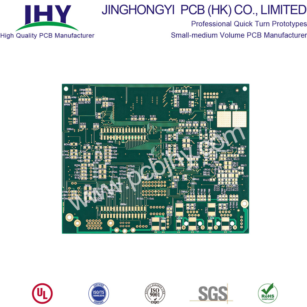
12 layer PCB Features and benefits
- Lead-free surface finish and lead-free components
- Long storage time (vacuum and anti-static packaging)
- Improved the speed of signal transmission
- Fast on time delivery
- UL certified and RoHS compliant
- Prototype PCB manufacturing
12 layer PCB Application
DSL Modem, Solar Battery Charger, Vehicle Tracker, GPS Receiver, Wi Fi Antenna, Bluetooth USB Hub, USB Wireless Router, SMS Modem, Multicoupler Antenna, Phone systems.
Printed Wiring Board,Custom Printed Circuit Board,12 Layer PCB,Custom 12 Layer PCB
JingHongYi PCB (HK) Co., Limited , https://www.pcbjhy.com